
Diamond Foundry Grows World's First 200 mm Single-Crystal Diamond Disk
The monolithic crystal aims to dissipate heat in high-power microchips and advance power electronics
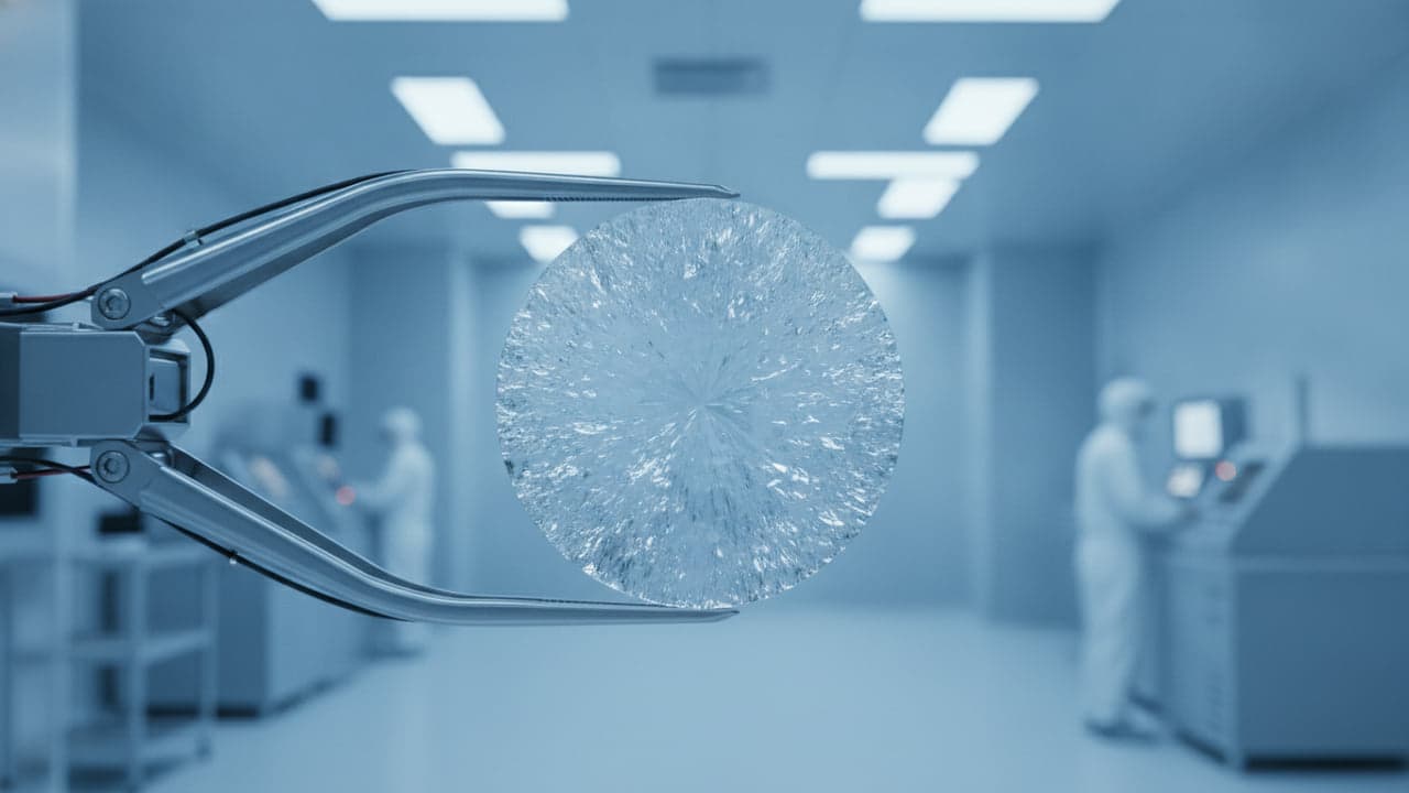
Diamond Foundry produced a 200-millimeter single-crystal diamond disk in an unpolished state, presenting the material on November 6 as the result of a 25-year research effort. The San Francisco company developed the continuous crystal to help pull heat away from high-performance microchips, particularly processors handling intensive artificial intelligence computations. Measuring 7.9 inches across, the monolithic sample represents a major technical invention in synthetic diamond synthesis.
Continuous crystal lattice replaces tiled segments
Growing diamond crystals at semiconductor dimensions has long posed severe physical hurdles. Natural and synthetic diamonds consist of carbon atoms bound in a strict lattice, and any defect in that grid interrupts heat transmission and electron flow. According to reporting by Interesting Engineering, earlier efforts to produce large diamond substrates relied on assembling smaller crystals together or using polycrystalline discs, which contain internal grain boundaries that trap heat. Overcoming these limits with a single-crystal wafer represents a major invention for the semiconductor industry.
The 200 mm sample created by the company is a single continuous structure without joined edges. Previously, Diamond Foundry fabricated 100 mm discs using diamond heteroepitaxy, a method where diamond crystals grow on an underlying foreign material while retaining an ordered lattice. While the firm has not specified whether the new 200 mm specimen relied on the identical growth mechanism, Chief Executive Officer Martin Roscheisen credited the achievement to combined advances in plasma physics, reactor design, crystal engineering and growth chemistry. He pointed to foundational work begun a quarter century ago by researchers Stefan Gsell and Martin Fischer.
Handling heat in dense processor packages
Thermal management has become one of the main physical limits for modern computing hardware. Modern chip architectures pack electrical circuits tightly—especially in power-hungry artificial intelligence systems—producing localized hot spots that throttle performance and degrade electronic components over time. High-purity single-crystal diamond offers a thermal conductivity of roughly 2,000 watts per meter-kelvin at room temperature, which is several times higher than copper.
Because of that thermal performance, single-crystal diamond can function as an effective heat spreader or substrate directly beneath active silicon dies, as noted by Interesting Engineering. Diamond also possesses a wide bandgap of about 5.47 electron volts. That wide bandgap makes the mineral suitable for high-voltage and high-frequency power electronics that must operate in severe electrical conditions without breaking down.
From rough sample to production wafer
The current unpolished disc serves as a development prototype rather than a finished commercial product ready for cleanrooms. To enter chip fabrication lines, manufacturers must polish the rough material, guarantee uniform thickness across the 7.9-inch diameter, and keep defect densities extremely low. Doping diamond with impurities to control its electrical conductivity also remains difficult, leaving diamond as a companion thermal material rather than a direct replacement for silicon.
Backed by its proprietary patent portfolio, Diamond Foundry reported that the 200 mm size makes a future 300-millimeter wafer predictable, though it has not shared a release date or manufacturing data for that diameter. To scale up industrial output, the firm is preparing a 2.77 billion dollars manufacturing facility in Spain supported by the European Chips Act, seeking to supply continuous diamond substrates to commercial semiconductor foundries.
Read also on The Patent: Pulsed 3D Printing Produces Meter-Long Single Crystals for Extreme Heat · Produced a super aluminum 25 times longer life